Redesigning the LM741-OP AMP using discrete components
Motivation
I have a bunch of BJTs and MOSFET transistors lying around in my special drawer. I thought it would be cool if I could assemble these components to remake the all-popular LM741 integrated operation amplifier in a breadboard. The catch will be that I explain all the circuit theory that is used to describe the functionality of each and every block. This is an excellent exercise, in my view, that would force me to master the theoretical knowledge, and the practical design considerations. It also emphasizes simulation in LtSpice and sometimes in MATLAB.
Analysis
The LM741 has quite complicated circuitry, the analysis of which will be extremely complicated if working with first principles. To simplify the analysis, it is useful to think of the overall opamp as consisting of an interconnection of several stage each of with defined standalone characteristics and relation with linked circuitry. Functionally, we need biasing circuitry throughtout the op amp to enable correct small signal operations. We need voltage gain stage that will amplify the small signal input voltage by some good amount. We need an output stage to provide enough output power for the op amp to drive loads.
Biasing
Working with BJTs, we have three regions of operation. The cutoff region is useless for voltage amplifying applications as the transistors is simply off, the saturation region is also useless since any incremental change in \(V_{BE}\) essentially results to no change in \(I_{D}\), on the other hand, in the active region, despite the exponential dependence of the collector current to base-emitter voltage, in the infinitesimal, applying a small incremental voltage in addition to the active-bias voltage, leads to a proportial incremental increase in the collector current in addition of the active-bias collector current and thus enables us to define the gain of the amplifier in terms of how much this proportional increase is. Biasing several transistors by applying a \(V_{BE}\) would require a many voltage sources attached to all these transistors, or a a common voltage with several voltage dividing resistors, all too inefficient. The use of current mirror circuits shines in this scenenario as they enable us to mimic some reference collector current to some other transistors with a factor dependent on the relationship between their process technology parameters (the emitter-base junction areas of the two transistors in this case).
We first create a current source using diode connected pnp and npn transistors with their collectors linked via a resistor \(R1\) using the schematic shown below:
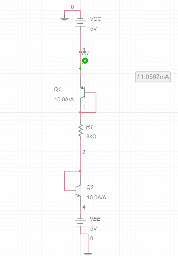
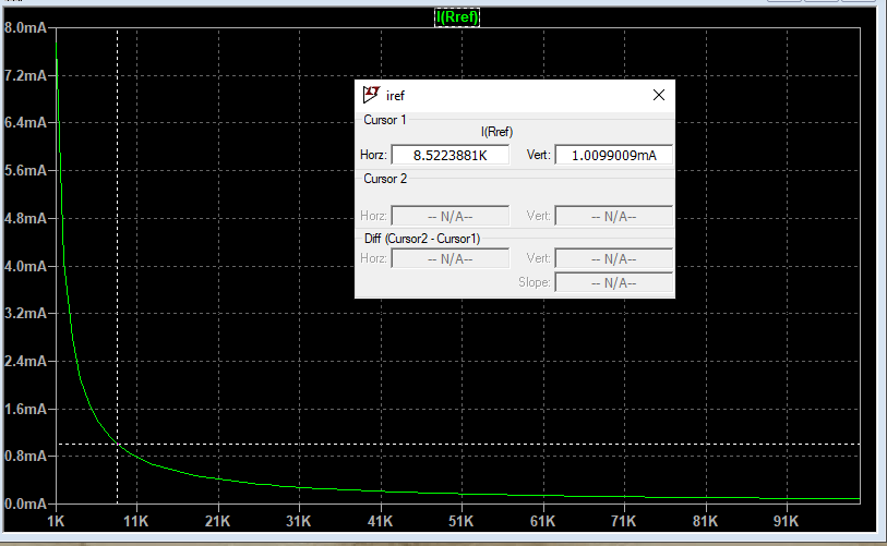
To determine the amount of the reference current \(I_{REF}\), we first consider what the base emitter voltages will be for the two transistors Q1 and Q2. Since the collector currents of both Q1 and Q2 are exponentially dependent on \(V_{BE}\) and the same current has to flow through both resistors, this necessarly implies that \(V_{BE1} = V_{BE2}\) . Furthermore, since \(V_{BE}\) is a logarithmic function of the collector current, with \(I_{REF}=1mA\) we can calculate the corresponding \(V_{BE}\) voltage using \(\begin {equation} V_{BE}=V_T ln(I_{REF}/I_S) \end {equation}\) where \(I_S\) is the saturation current and \(V_T\) the thermal voltage, the value of \(V_{BE}\) can be calculated to be approximately 0.7V. This assumption is useful in the design of current source because now we can write a voltage loop equation to solve for \(I_{REF}\) i.e \(V_{CC} - V_{BE} - I_{REF} R1 -V_{BE}+V_{CC}=0\) which simplifies to \(\begin{equation} I_{REF}= 2(V_{CC}- V_{BE})/R1 \end {equation}\). Note that the collector base voltage drop \(V_{CB}\) is zero in both transistors as they are diode-connected(base and collector are short-circuited). The positive and negative power supply voltage is assumed to equal in magnitude and our assumption \(V_{BE}=0.7V\) is justified by a proper choice of \(R1\) that would give the current \(I_{REF}=1mA\) . Alternatively, we could figure out the exact value of \(I_{REF}\) and \(V_{BE}\) using the load-line method for which the operating point is the intersection of the resistor IV curve and the two transistor’s IV curve. The downside of this method is that we need to know the resistor value before-hand or otherwise determine by iteration. In LTspice we can simulate the reference current source circuit over a range of different \(R1\) resistor values using the netlist below:
**power supplies
vss vss+ 0 dc 20
vee vee+ 0 dc -20

**Diode connected transistors
qq1 cnode cnode vss+ 2N5087
qq2 cnode2 cnode2 vee+ 2N5088

**resistor
rref cnode cnode2 {var_r}

.include 2N5087.lib
.include 2N5088.lib

.step param var_r 1k 100k 1k
.op

.end
By plotting the current over a range of \(R1\) values, we determine that a resistance of around \(R1=8k\Omega\) is needed to pass 1mA of current for our reference current.
The convinince of using Q1 transistor in the design of the current source is that we are able to source an extra current steering circuit on top of the diode-connected Q2 transistor. Since a BJT transistors can be modelled using current sources, resistors and diodes, it is understood that the short-circuiting the collector and base results reduces the transistor model to a diode model which is a voltage dependent current source controlled by \(V_{BE}\). You can see this in the npn transistor model shown below:
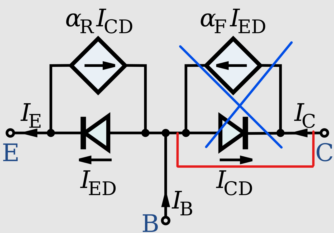
Additionally, the base-collector short circuit ensures that the transistors is always in the active region as \(V_{BE(0.3V)}> V_{CE_sat (0.3V)}\) . Once \(V_{BE}\) is established in transistor Q1, the parallel connection to transistor Q3 would ensure that \(V_{BE3}=V_{BE2}\) if resistor \(R_e=0\) and in turn \(I_{REF}== I_{D3}\) would hold if the transistors are identical (thus the current mirroring action). The addition of the resistor at the emitter of the Q3 is a special current source i.e. “Widlar current source”. This current source introduces an advantage over the conventional current mirror circuit which is allowing the magnitude of resistor \(R1\) to be reduced and still get a well defined current in Q3 using the formula \(\begin {equation} I_3 R3 =V_T ln(I_3/I_{REF}) \end {equation}\)